PCB or printed circuit board is undoubtedly the most important element of the whole electronics industry. If you have mastered this complicated circuit board, you are now on the top of entire industry.
Whether you want to do it to start your own PCB business or just for educational purposes, you can’t master this thing until you know the whole manufacturing process.
Hence, we are here with everything you need to know about manufacturing PCB from designing to finishing. So, let’s go:
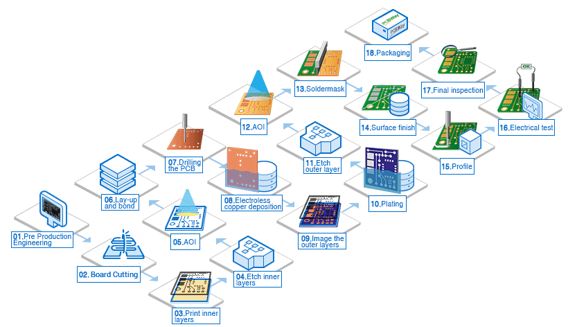
Step-by-step Process of Manufacturing of the PCB Step 1: Designing Process
Before anything else, PCB is first designed using any PCB design software like Eagle or OrCAD. It’s always better to tell manufacturer about the version of software that’s used to design PCB to eliminate any problems that can happen in future.
Every calculation and information should be taken precisely. Once the designer is satisfied with the design, he should hand over the blueprint to manufacturer so that he can do the rest. Moreover, manufacturer has to use film to create an image of PCB for easier process.
Step 2: Reviewing and Questioning
If you are not engineer, you have to hire one because he’ll review the design to meet the requirements. Engineers usually ask themselves, designer, and manufacturer questions like these:
- Will design become problematic while manufacturing?
- Is the design error-free?
Step 3: Printing the PCB Design
It’s time to print the inner layer of PCB!
In this process, plotter printer will be used which is indeed a laser printer but the one that follows much more precise instructions. Different colors have to represent different portions of the design for example, conductive copper traces will be represented using black-colored ink.
Step 4: Play With Copper and Remove It
It’s time to play with copper!
It’s a bit complicated process but still one of the favorite steps of many manufacturers. Here, copper foil layer will be applied to PCB design that has been printed. Then copper is again pre-bonded to the laminate (structure of PCB design). Now, chip away copper to reveal blueprint of design.
Cover the design with photo-sensitive film (resist) and wait for it to receive as much UV light through pores as possible. It’s to let it dry.
Step 5: Layer Alignment and Optical Inspection
After cleaning and making them ready, it’s time to align the layers. Now, technician will carefully place the layers in optical punch (machine). It’s done to ensure layers are aligned and punched perfectly.
Step 6: Lamination Process
Laminate the layers so that they can stay together for long. The outer layer of board is made of fiberglass that’s soaked in or coated with epoxy resin. It means that you can easily sandwich layers of PCBs on a special lamination table.
Step 7: Drilling
Use X-ray machine to locate points where you have to drill the board. After determining spots, use computer-guided drill to do the job. During or after drilling, excessive copper will also get settled from the edges.
Step 8: PCB Plating
In plating process, a special chemical is used to temper different layers of PCBs together. Clean and bathe the board thoroughly using chemical and extremely thin layer of copper. Make sure computer is controlling all the processes for precise results.
Step 9: Outer Layer Imaging
Just like before, a layer of photoresist is again applied (only on outer layer) to attract UV light for better imaging. This step is pretty much same as the step 4, so do it but with more precision and accuracy.
Step 10: Etching
Etching process is complicated because while etching, there’s always a fear of copper layer coming off. So, a thin layer of tin is used as a guard for copper. This process is done by engineer who gets rid of unwanted material (even a slight amount of surplus copper).
Step 11: Solder Mask Application
Clean the both sides of board thoroughly before covering them with an epoxy solder mask ink. Then, put a huge amount of UV light on the board all of a sudden so that it can become a bit harder. Ink prevents specific parts from getting hard.
Step 12: Finishing and Ink-jet Writing
Chemically plate PCB with gold or silver and run any surface finishing process as suggested by your customer. After that, perform ink-jet writing which is called silkscreen. This step will ensure that all vital information is there on the board.
Step 13: Tests and Quality Checks
Call the technician for simple electrical tests. After that, perform profiling and V-scoring to make PCBs ready for cutting. After cutting, deliver them to the client.
Final Takeaway
PCB manufacturing is usually taken as a quite lengthy and complicated process. But here, we’ve tried our best to convey the message as shortly as possible. So, that was the easiest step-by-step procedure to manufacture your first cluster of PCBs.
For more information about PCB manufacturing, click here!


